電磁波解析(ナノ構造)ナノ凹凸構造によるLEDの光取り出し効率改善
Abstract
電磁波解析ソフトKeyFDTDを使用してナノ凹凸構造によるLEDの光取り出し効率改善のシミュレーションを行った。 LEDは旧来の白熱電球などと比較して、耐久年数や発光効率に優れている。 LEDの発光効率改善には、LEDに流す電流に対し、LED内で発生する光子の個数の割合を示す内部量子効率、発生した光がLED外へ出る割合を示す光取り出し効率、その他基板等の改善が挙げられている。 光取り出し効率を改善する技術に可視光に対してサブ波長にあたるナノ構造を表面に付与する手法がある。 本報告書では複数形状のナノ凹凸構造をFDTD法でシミュレートし、光取り出し効率が改善されることを確認した。
Simulation of the improvement of light extraction efficiency of LED by nano-uneven structure was carried out by using the electromagnetic analysis software KeyFDTD. Compared to conventional incandescent light bulbs, LEDs are superior in terms of durability and luminous efficiency. The improvement of LED luminous efficiency includes internal quantum efficiency, which indicates the ratio of the number of photons generated in the LED to the current flowing through the LED, light out-coupling efficiency, which indicates the ratio of the generated light going out of the LED, and other improvements in the substrate, etc. A technique to improve the light out-coupling efficiency is to add sub-wavelength nanostructures to the surface of visible light. In this report, the FDTD method was applied to simulate the nano-uneven structure of multiple shapes and the improvement of the light out-coupling efficiency was confirmed.
1. 解析概要
LEDの発光効率改善には内部量子効率、光の取り出し効率、その他基板等の改善の3つが挙げられている[1] 。光取り出し効率を向上させる技術にナノ構造を表面に付与する手法がある。本報告書ではナノ凹凸構造付与する場合と付与しない場合をFDTD 法によりシミュレートして比較し、ナノ凹凸構造による光取り出し効率の改善効果を報告する。
There are three types of improvements in the luminous efficiency of LEDs: internal quantum efficiency, light extraction efficiency, and other improvements such as the substrate [1]. One of the technologies to improve the light out-coupling efficiency is to add nanostructures to the surface. In this report, the FDTD method is simulated and compared with and without the nano-convex structure, and the effect of the nano-convex structure on the light out-coupling efficiency is reported.
2. 解析条件
Fig.1に解析モデルを示す。
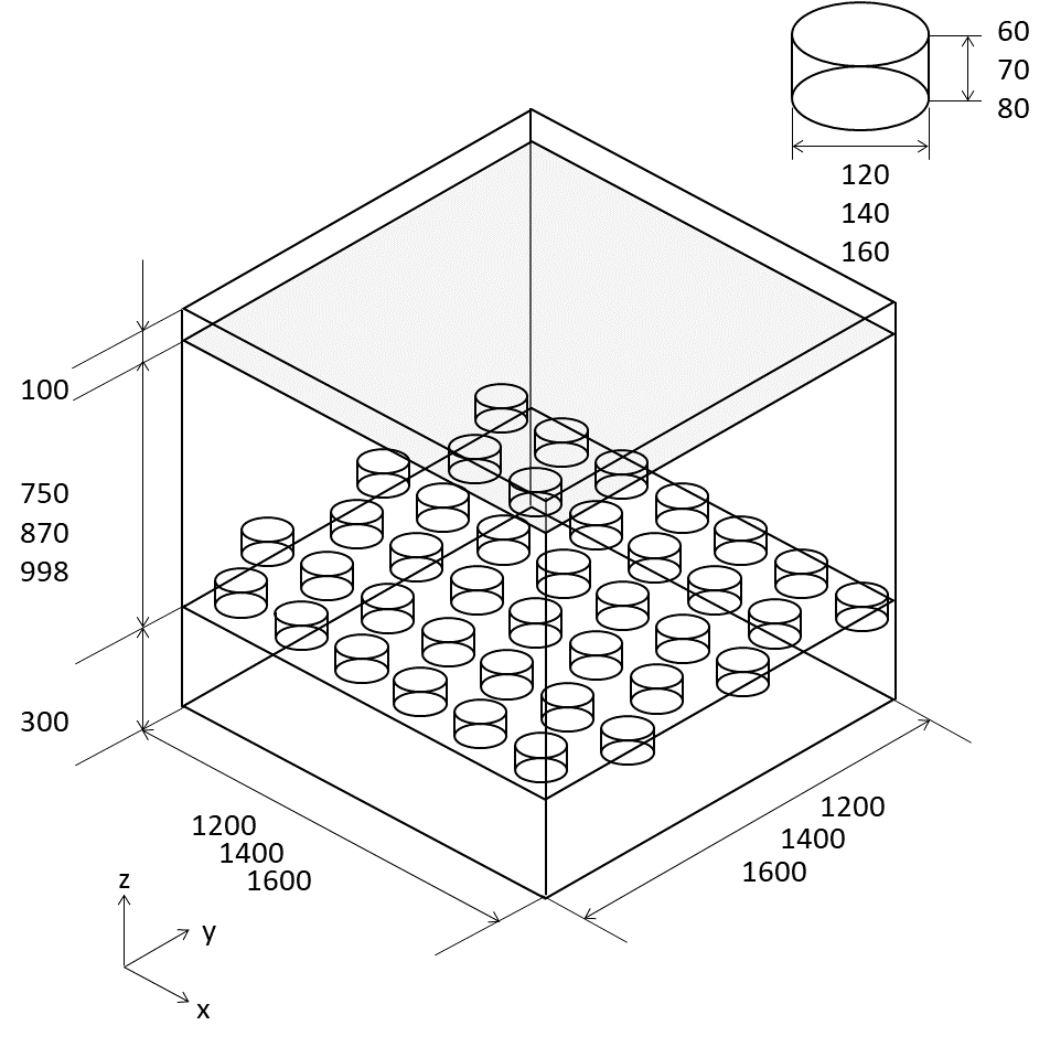
Fig.1 Simulation model
境界条件は全て吸収境界PMLを適用した。誘電体表面から1波長以上離した位置で、x、y方向解析領域と同じ大きさの面を+z方向に通過するポインティングベクトル(以下Sz)の1波長積算値総和を求め、ナノ凹凸構造の有無におけるSzの比から取り出し効率の改善率を導出した。
屈折率3.2の誘電体内にx方向励振の点源を配置し、Fig.1中のSz取得位置までの距離、ナノ凹凸形状、周期を1倍、1.16倍、1.33倍とした場合の波長350~750[nm]における光取り出し効率改善率の周波数特性を導出した。
3. 解析結果
Fig.2に波長350~750[nm]における3形状のナノ凹凸構造による光取り出し効率の改善率を示す。各形状で改善率は最大約1.5倍、改善率のピーク波長は1倍で500[nm]、1.16倍で600[nm]、1.33倍で750[nm]であった。3形状の改善率ピーク波長におけるナノ凹凸構造断面部の電界分布をFig.3~5に示す。ナノ凹凸構造内の定在波は3形状で類似していることからナノ凹凸構造の形状、配置によりFig.3~5に類似した定在波となる周波数範囲で高い改善率を示すと考えられる。また、ナノ凹凸構造とピーク波長の比率の不一致は点源の位置が構造に比例していないため、点源から界面までの距離を比例させることで異なるピーク波長を示すと考えられる。
The improvement rate of light out-coupling efficiency by nano-uneven structure was investigated by using the electromagnetic wave analysis software KeyFDTD. It was confirmed in the simulation that the extraction efficiency was improved by a maximum of 1.5 times by the nano-uneven structure and that the peak wavelength of the improvement rate varied with the structure and period.
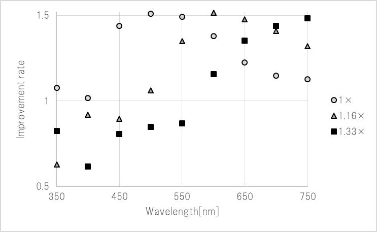
Fig.2 Improvement rate of Light extraction efficiency
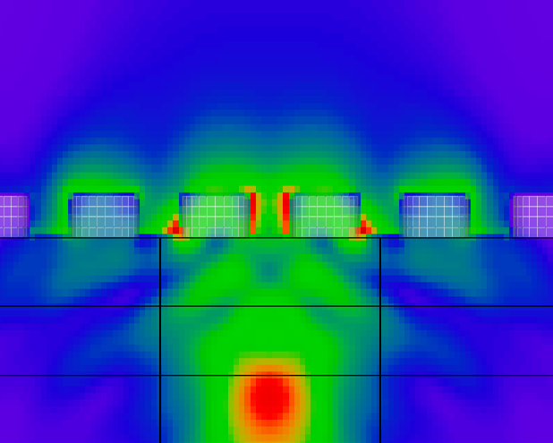
Fig.3 Electric field distribution(×1 : λ=500[nm])
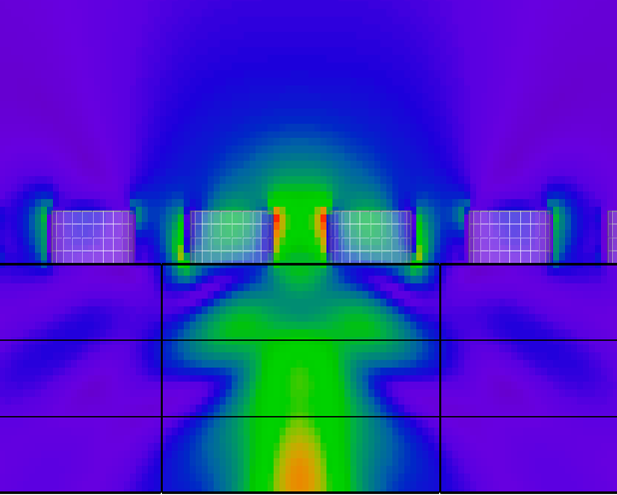
Fig.4 Electric field distribution(×1.16 : λ=600[nm])
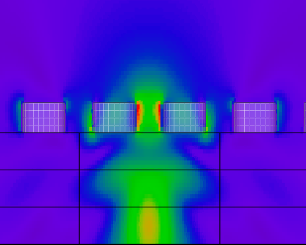
Fig.5 Electric field distribution(×1.33 : λ=750[nm])
Fig.4 Electric field distribution(Diameter=80[nm])
4. まとめ
電磁波解析ソフトKeyFDTDでナノ凹凸構造による光取り出し効率の改善率を検討した。ナノ凹凸構造により取り出し効率が最大1.5倍改善する点と構造、周期により改善率のピーク波長が変化する点がシミュレーションで確かめられた。
The improvement rate of light out-coupling efficiency by nano-uneven structure was investigated by using the electromagnetic wave analysis software KeyFDTD. It was confirmed in the simulation that the extraction efficiency was improved by a maximum of 1.5 times by the nano-uneven structure and that the peak wavelength of the improvement rate varied with the structure and period.
お問い合わせ・資料ダウンロード・入門動画視聴のお申し込みはこちら
お問合せフォームを開く