電磁波解析(ナノ構造)金ナノワイヤーの電磁波解析
Abstract
金ナノワイヤーは、ベンゼン環を含む化合物の酸化触媒として金ナノ粒子よりも活性が高いことが報告されている。この触媒活性の起源を調査するために、電磁波を入射した際の金ナノワイヤーの周辺の電界分布をFDTD法で計算した。
Gold nanowires have been reported to be more active than gold nanoparticles as catalysts for the oxidation of benzene ring-containing compounds. In order to investigate the origin of the catalytic activity, the electric field distribution around the gold nanowires was calculated by the FDTD method when the electromagnetic waves were injected.
1. 解析概要
金ナノワイヤーとは直径数[nm]、長さ数[µm]の円筒状のナノ物質であり、ベンゼン環を持つ化合物の酸素酸化触媒として通常の金ナノ粒子より高い触媒性能を持つことが報告されている[1]。このナノワイヤーの触媒性能の起源について調べるために、金ナノワイヤーに300 [THz]の電磁波を入射した際の電界強度を、電磁波解析ソフトKeyFDTDを用いて解析し、金ナノワイヤーのどこに触媒活性が期待されるか、また金ナノワイヤー同士を近接させた場合にどのように電界強度が変化するかを調べた。
Gold nanowires are cylindrical nanomaterials of several diameters [nm] and lengths [µm] that have been reported to have higher catalytic performance than ordinary gold nanoparticles as oxygen oxidation catalysts for compounds with benzene rings [1]. In order to investigate the origin of the catalytic performance of the gold nanowires, the electric field strength of the gold nanowires when an electromagnetic wave of 300 [THz] is injected into the gold nanowires was analyzed by using the electromagnetic wave analysis software KeyFDTD to find out where the catalytic activity of the gold nanowires is expected and how the electric field strength changes when the gold nanowires are close to each other.
2. 解析条件
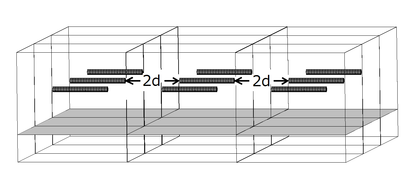
図1に解析モデルを示す。

図1 金ナノワイヤーの解析モデル
可視光帯における金の物性はDrude-Lorentz-Lorentzモデルを用いて近似した[2]。x,z方向を周期境界条件に設定したため図2に示すように金ナノワイヤーが軸上に近接している。そこでワイヤー同士が近傍に存在するときの影響を調べるために、金ナノワイヤー間のx方向の距離2dについて100 [nm] (解析a) と10 [nm] (解析b) の2つのパターンに分け、それぞれ金ナノワイヤーの辺と入射光の電界成分が平行な場合と、磁界成分が平行な場合について電界強度の分布を調べた。但し金ナノワイヤーの長さを一定にして距離dを変化させるために、解析領域とメッシュを解析aと解析bで変更した。
| 金ナノワイヤー | 直径: 10[nm]、長さ:100[nm] |
|---|---|
| 励振源 | 300[THz]、sin波 |
| 物性 | 金:Drude-Lorentz-Lorentzモデル |
| 解析領域a | 200×200×200[nm] |
| メッシュa | x:100、y:100、z:100 |
| 解析領域b | 110×200×200[nm] |
| メッシュb | x:55、y:100、z:100 |
| 境界条件 | x、z: 周期境界条件、y:吸収境界条件MUR1 |
| タイムステップ | 3.34e-18[sec] |
3. 解析結果
図3、4から解析a、bともに、金ナノワイヤーと磁界成分が平行の場合には強い電界は現れなかったが、電界成分が平行の場合にはナノワイヤーの両端に強い電界が確認された。これは金ナノワイヤーにおける電界成分の共振と考えられる。強い電界により原子間の電荷授受が素早く起こるとすれば、金ナノワイヤーを触媒として用いた際にワイヤーの両端が触媒活性点として振る舞う可能性がある。
図3、4の左図を比較すると、10 [nm]までワイヤーを近接させた場合は周期境界まで強い電界が現れており、ワイヤーの隙間全体が強い電界分布している。この現象に関してナノワイヤー間距離をパラメータとして定量化するには更なる解析を要する。

図3 電磁波解析a ( 2d=100 [nm] ) の結果(左 : 電界成分と平行、右 : 磁界成分と平行)
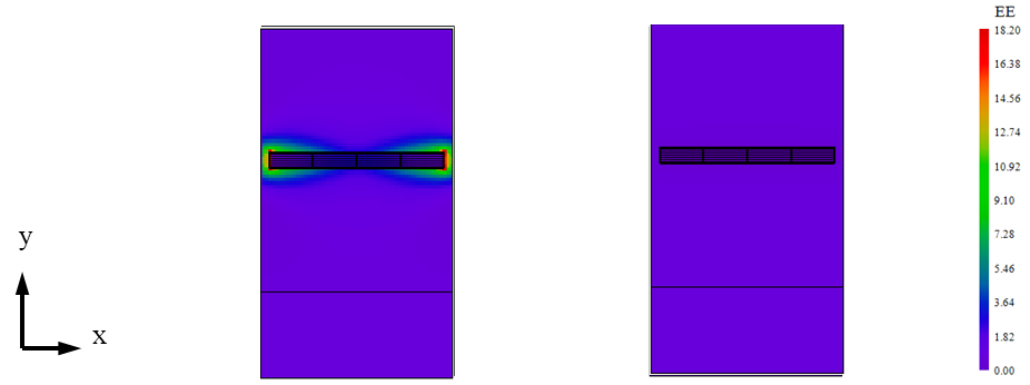
図4 電磁波解析b ( 2d=10 [nm] ) の結果(左 : 電界成分と平行、右 : 磁界成分と平行)
4. まとめ
本報告書では100 [nm]の金ナノワイヤーを対象とした。今後はナノワイヤー間距離やナノワイヤーの径、長さをパラメータとして比較・検討したい。
In this report, gold nanowires at 100 [nm] were targeted. In the future, it is desirable to compare and study nanowire distances and nanowire diameters and lengths as parameters.
[1] Hu, L. et al., Chem. Commun. 2011, 47, 1303.
[2] 株式会社 科学技術研究所 科学技術部, 金、銀、銅の反射シミュレーション, https://dev-www.kagiken.co.jp/analysis-keyfdtd/au-ag-cu-reflectance/
お問い合わせ・資料ダウンロード・入門動画視聴のお申し込みはこちら
お問合せフォームを開く